
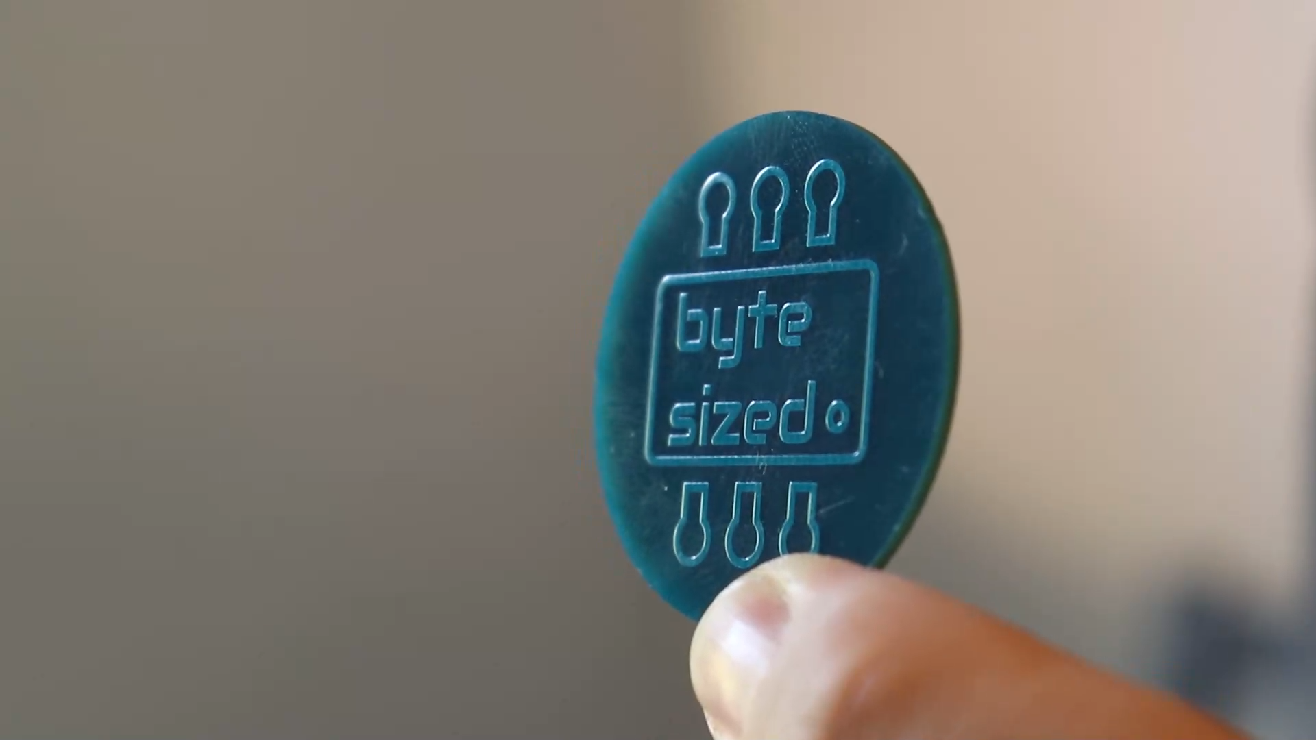
How To Make PCB Art
We all know the virtues of designing a printed circuit board for your electronics projects. There is no better feeling than taking a rat’s nest of wires on a breadboard and soldering the components to a professionally manufactured printed circuit board. Even the most ugly circuit prototypes can transform into a clean and reliable board that just works every time. No more finding rogue jumper wires and plugging them back into the breadboard! A while back I even made a video on how to make a functional custom PCB, but did you know that printed circuit boards can also be used as an art medium? It turns out it's way easier than I thought! I made a few boards for my favorite YouTube channel I Like To Make Stuff, as well as some Star Wars boards. These can be used on your keychain, or backpack, as christmas ornaments, or used in ways I haven’t even thought of yet! These boards don’t have any electronics on them, but there is no reason they can’t! Here is a step by step tutorial of how do make your own PCB art.
What are PCBs Made of?
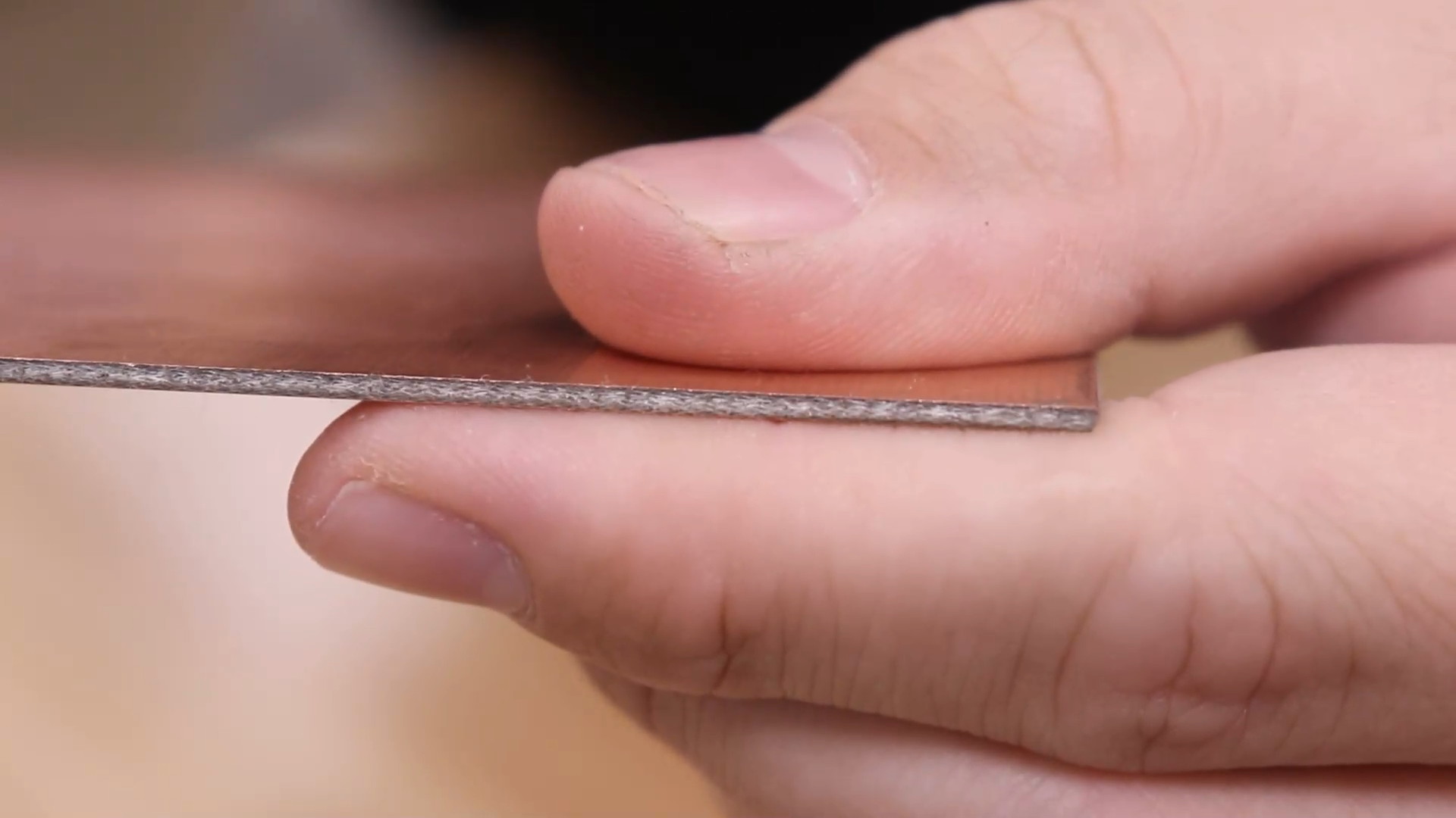
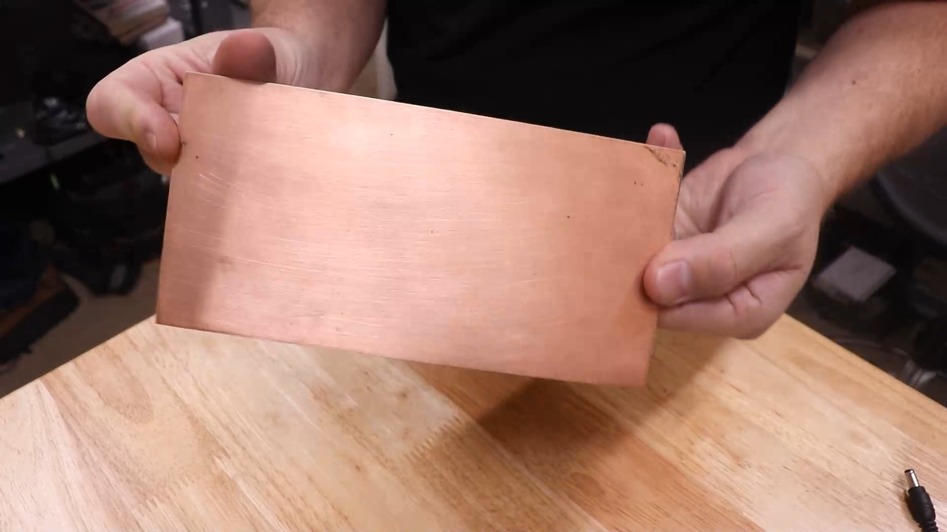
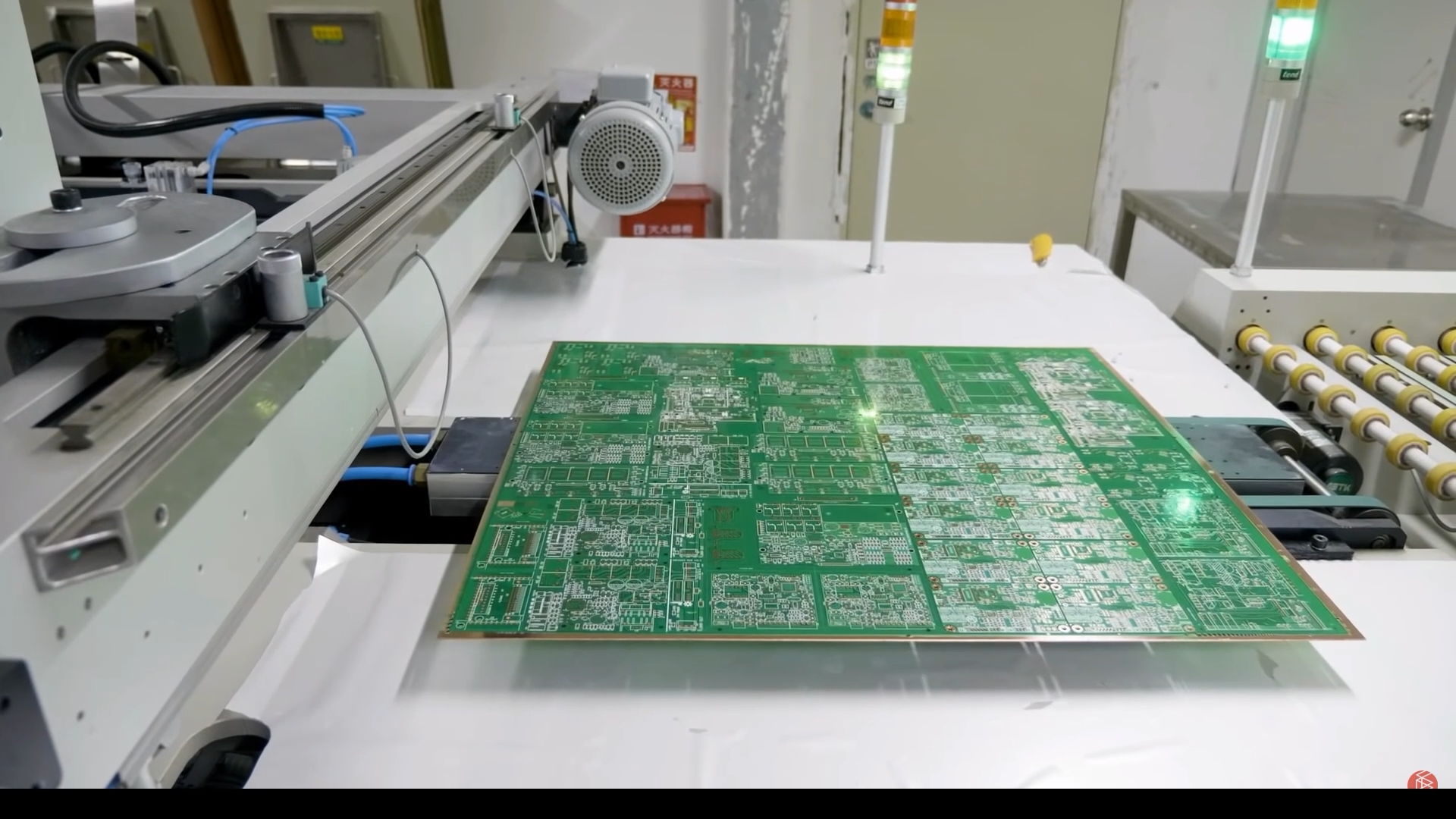
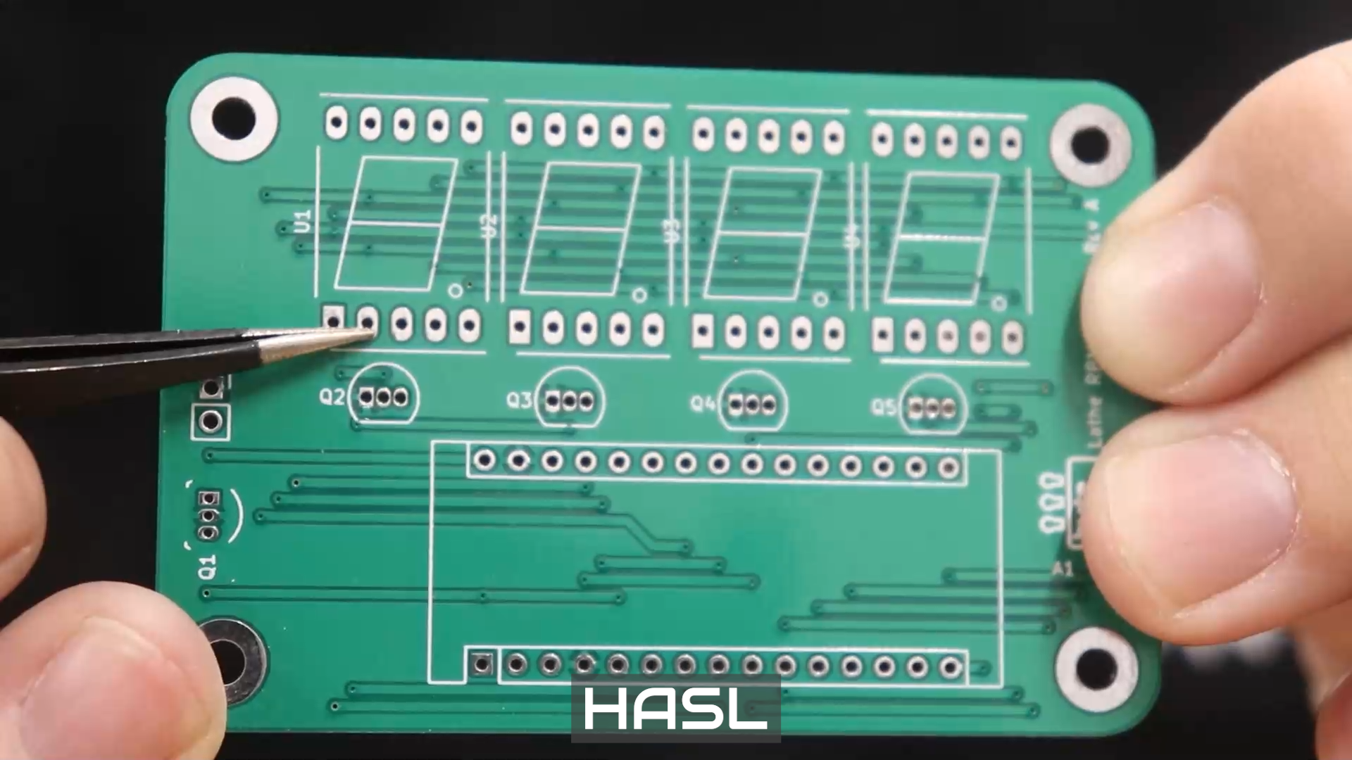
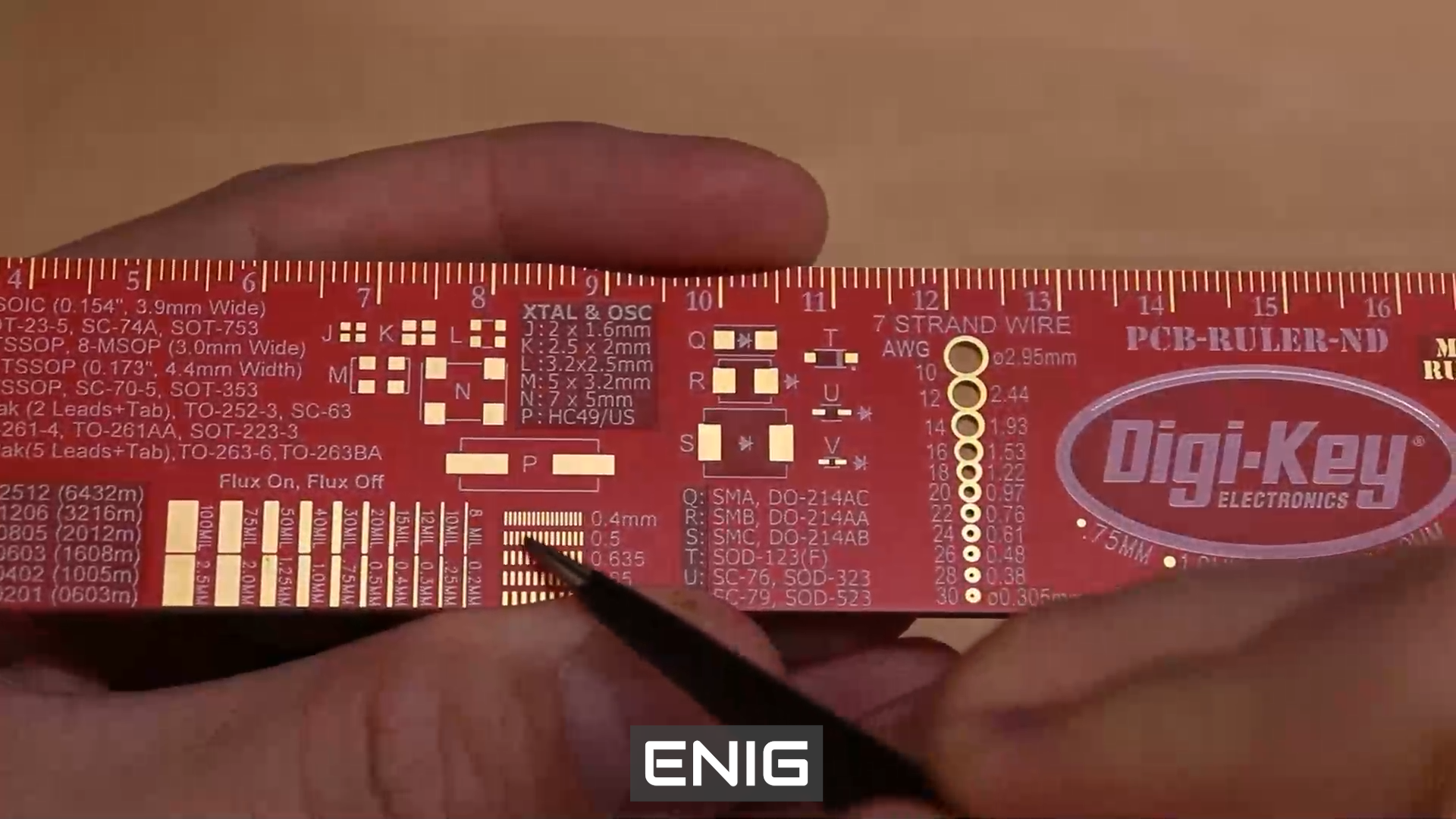
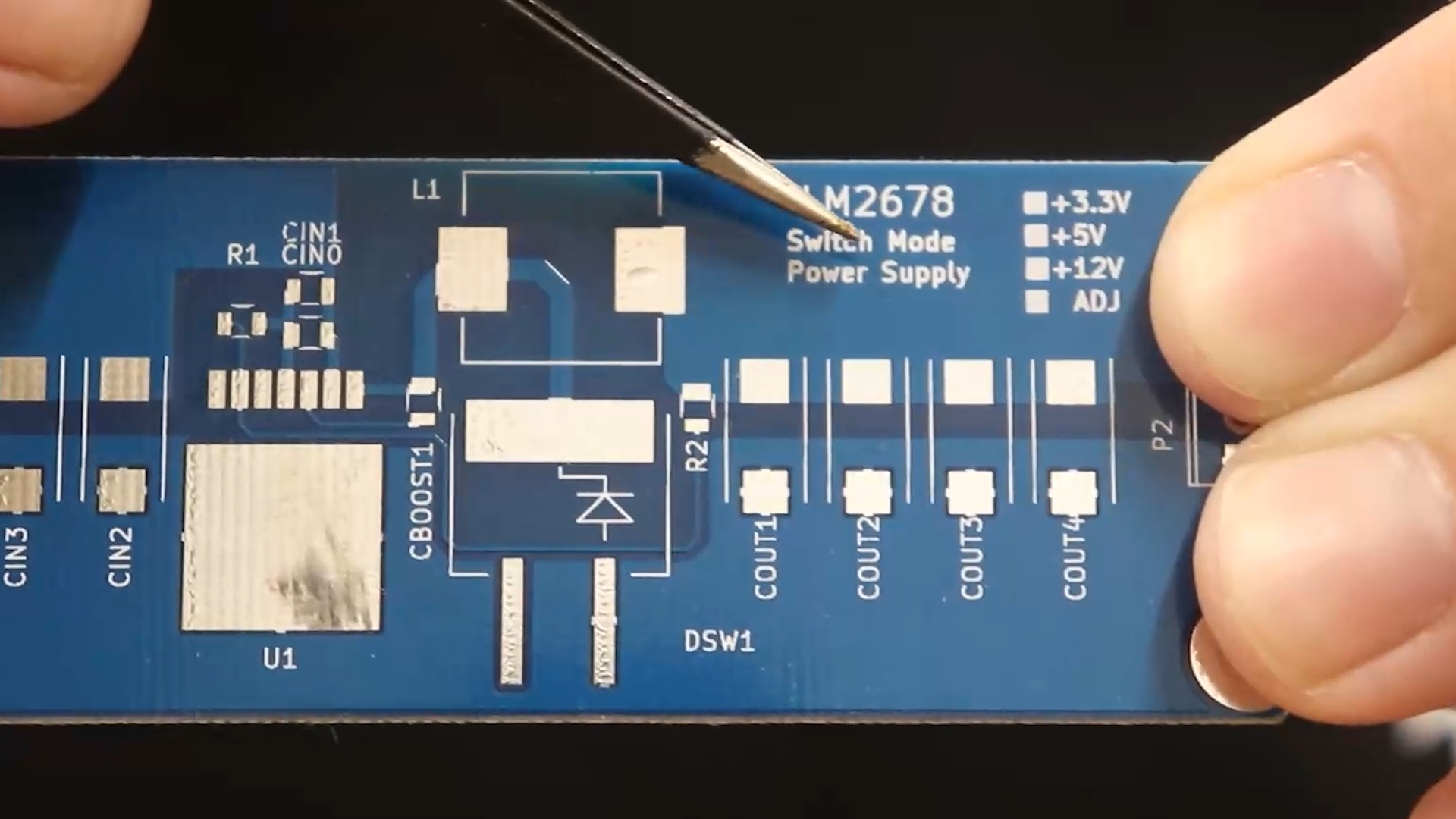
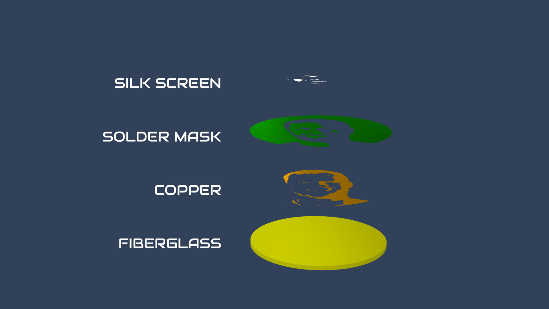

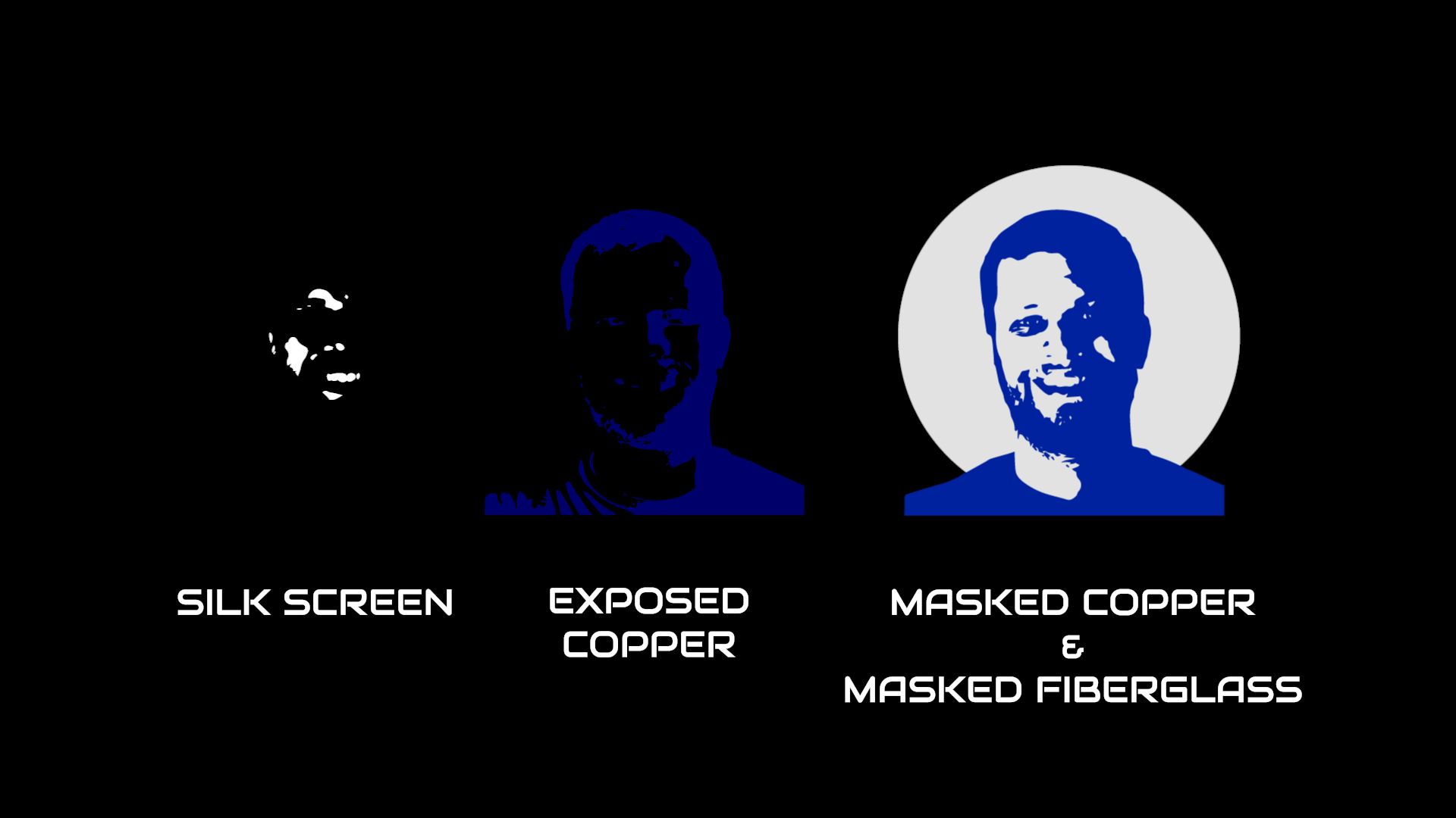
Printed circuit boards (PCBs) are made from different manufacturing layers. The base is usually a fiberglass sheet about 1/16” (1.6mm) thick covered with a thin layer of copper on one or both sides. A designer will create a board layout (sometimes called “artwork”) and send the design files to a board manufacturer. The manufacturer will use acid to etch the parts of the copper that are not needed leaving isolated traces, pads, and holes for the electrical components. From there they add a layer called the solder mask which is what gives PCBs their signature green color. Solder masks can be colors other than green of course. The mask is careful to leave small openings anywhere a component needs to be soldered to the board. Like most metals, copper oxidizes when left exposed to air and moisture. Any oxidation on the copper surface would prevent components from making a good solder connection so the manufacturer uses one of two process to protect the exposed copper pads. The cheaper default process is called HASL and it’s just a thin layer of melted solder applied to the copper pads. The more expensive and higher quality process is called ENIG which is a thin layer of gold applied to the copper pads. Both of these surface finishes protect the copper from oxidation and make the surface of the pads shiny. Finally a PCB would be hard to assemble and identify without some sort of markings for each component so the manufacturer uses a white ink in a silk screening process. Component identifiers, labels, revision numbers, company names and logos can all be applied to the board on the silk screen layer. The result of all these layers is a precise layout and connection of dozens or sometimes hundreds of component signals. The stacked layers create a beautiful color palette which starts with the darkest layer, the masked fiberglass. The layers get lighter with the masked copper and exposed tinned copper layers. The lightest layer is the silk screen layer. In order to create artwork from PCBs I will take advantage of those manufacturing layers and use them to represent the various parts of an image.
Image and software selection

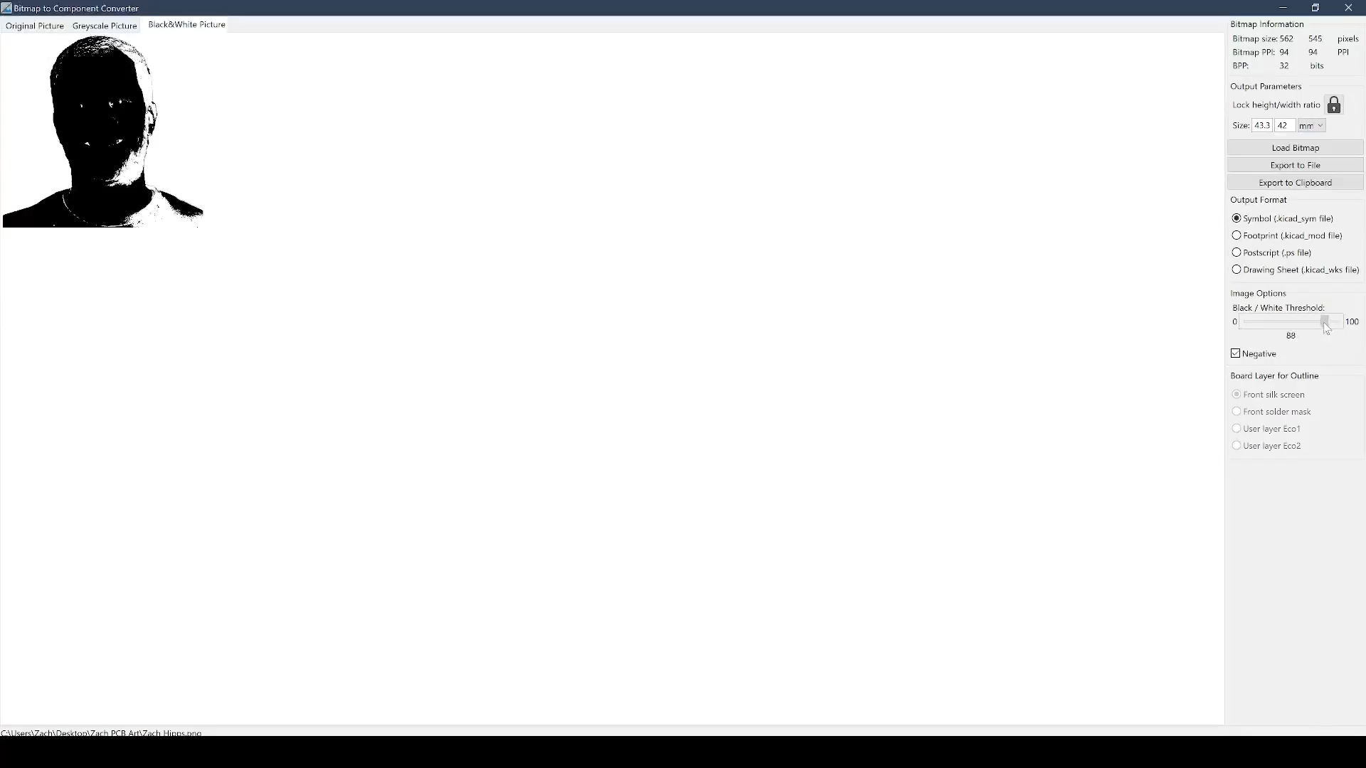
There are a lot of circuit board design software options out there. If you have a favorite I’m sure it’s possible to do these same steps, but for this tutorial I’ll be using KiCad which is an open source and free design environment. First I downloaded the latest release of KiCad and installed it on my computer. Next I looked through some potential images to create PCBs from. I wanted to start simple so I chose a profile picture of myself. It’s important to choose an image with lots of contrast and try to find one with a white background. You want a range from dark shadows to bright highlights and all the midtones in between. If you choose a flat image without much contrast this process won’t work as well. Once I had my image selected I opened the KiCad image converter tool and loaded my bitmap image. Within this tool there are color, greyscale, and black & white versions of my image. For the most part I’ll be using the black and white image tab to process the image into the different layers.
Creating PCB Layers
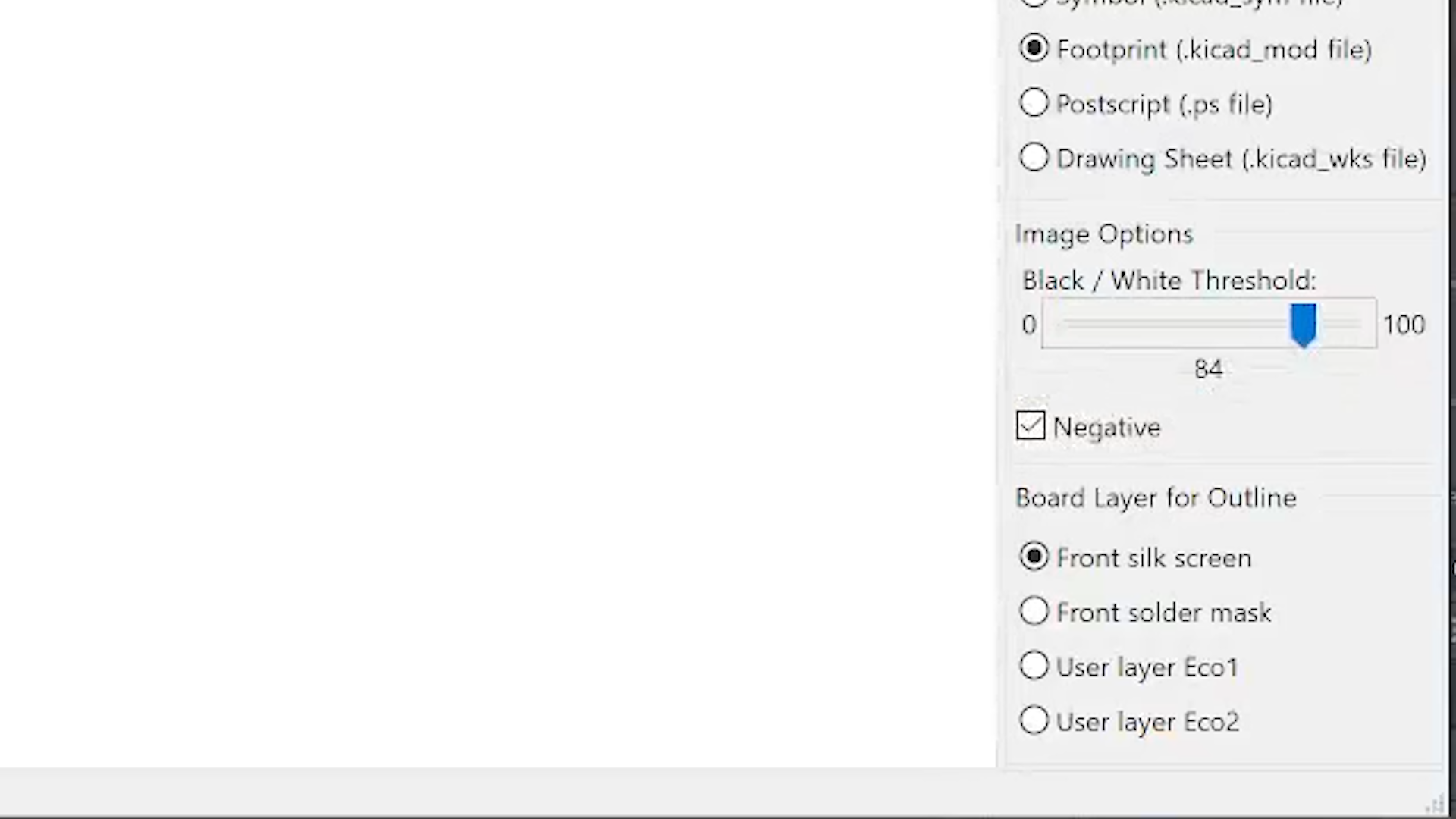
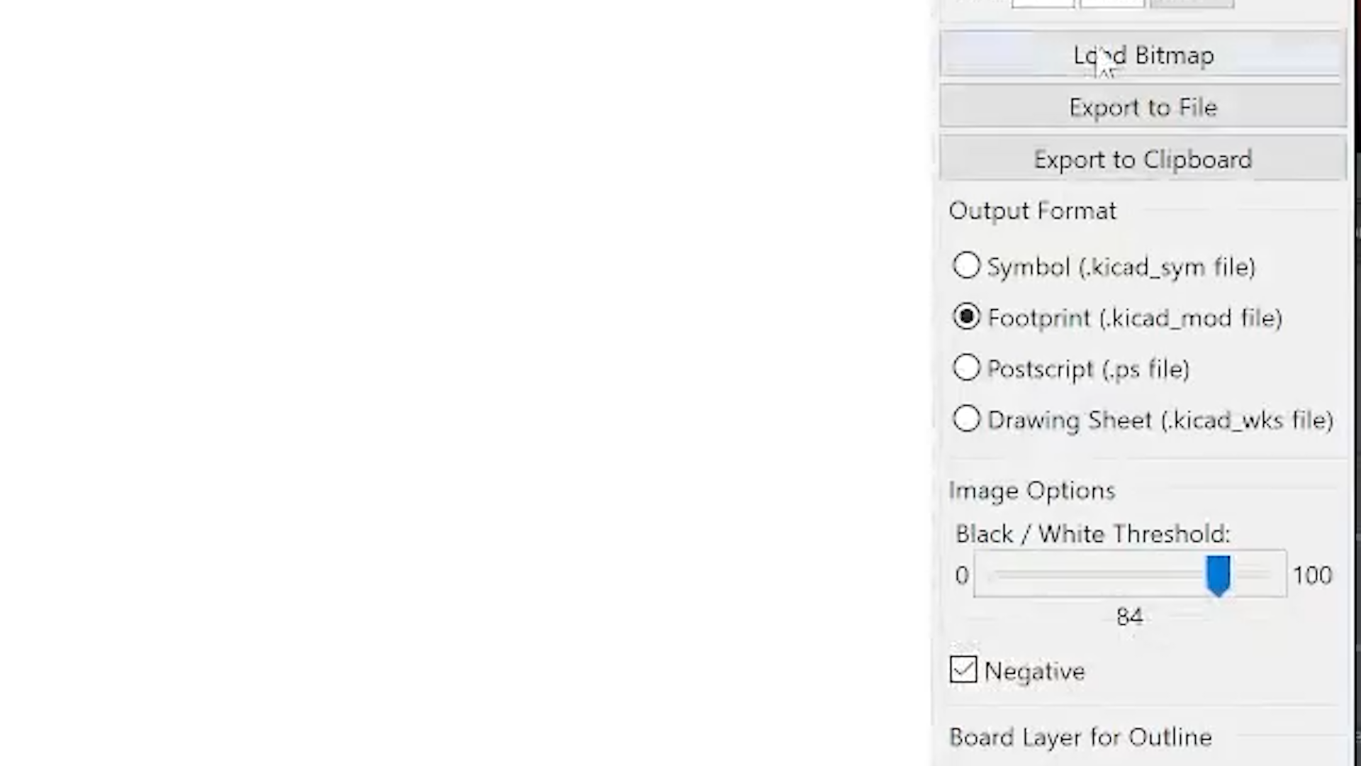
The first thing I need to do is use the output parameters to resize my image to be slightly larger than the PCB I want to make. If I make it smaller or even the same size the edges of the image may show up on the PCB and I don’t want that. Next, I select Footprint (.kicad_mod file) under output format. Lastly, I’ll check the negative box under image options and play around with the threshold slider to see how it affects the image. The masked fiberglass is the darkest so that will be the background of my image. Now I’m ready to create the masked copper layer so I need to isolate the darkest parts of my image from the background. I only want the darkest parts of my image so I will start at 100 and adjust the threshold down until the white pixels show the darkest parts of my face and everything else is shown as black pixels. The white pixels will become the masked copper on the PCB, but KiCad doesn’t have a way to export to the copper layer. I will show you how to fix that later, so for now I select “front silk screen” under the board layer for outline section and export the file. I named this layer F.Cu which stands for front copper. Next I want to create the exposed tinned copper layer so I need to isolate the next lightest parts of my image from the previous layers. I will slide the threshold down even further than before to reveal the midtones. The black pixels will be exposed tinned copper so once I am happy with the threshold value, I’ll select front solder mask under board layer for outline and export the file. I name this file F.Mask and save it alongside the first file. Now it’s time to move on to the highlights of my image so I move the threshold down even further until just the brightest parts of my image like my teeth and the shiny parts of my cheek are shown in black pixels. I think the images look best when the silk screen is used sparingly, I don’t want to go overboard here. With the threshold set for the highlights I select front silk screen under board layer for outline and export the file. This time I’ll name the file F.SilkS and save it alongside the other two files.
Creating the PCB
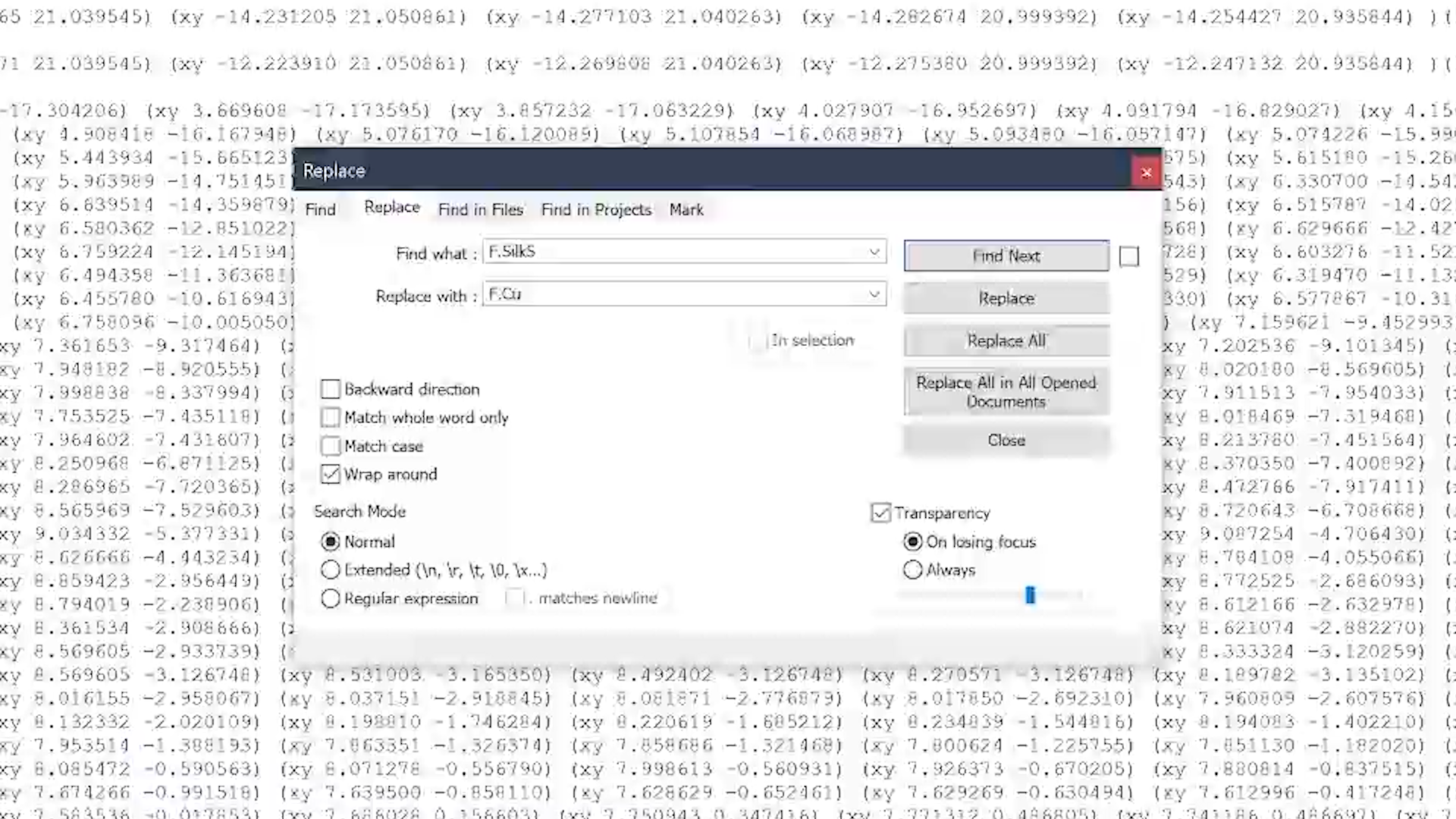
Before we can open the PCB editor in KiCad, we need to do a little cleanup on the three files we just created. Any plain text editor will work, but I use notepad++ to open all three files. These plain text files use a markup language to describe the polygons needed for each layer. The top of the file has a header followed by these two elements:
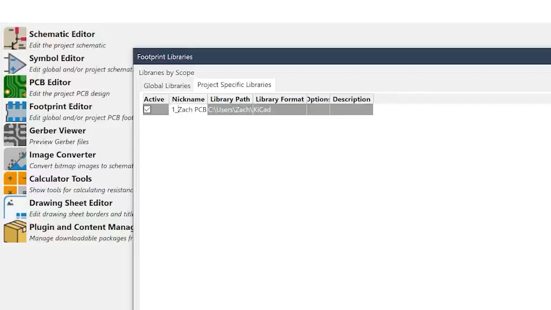
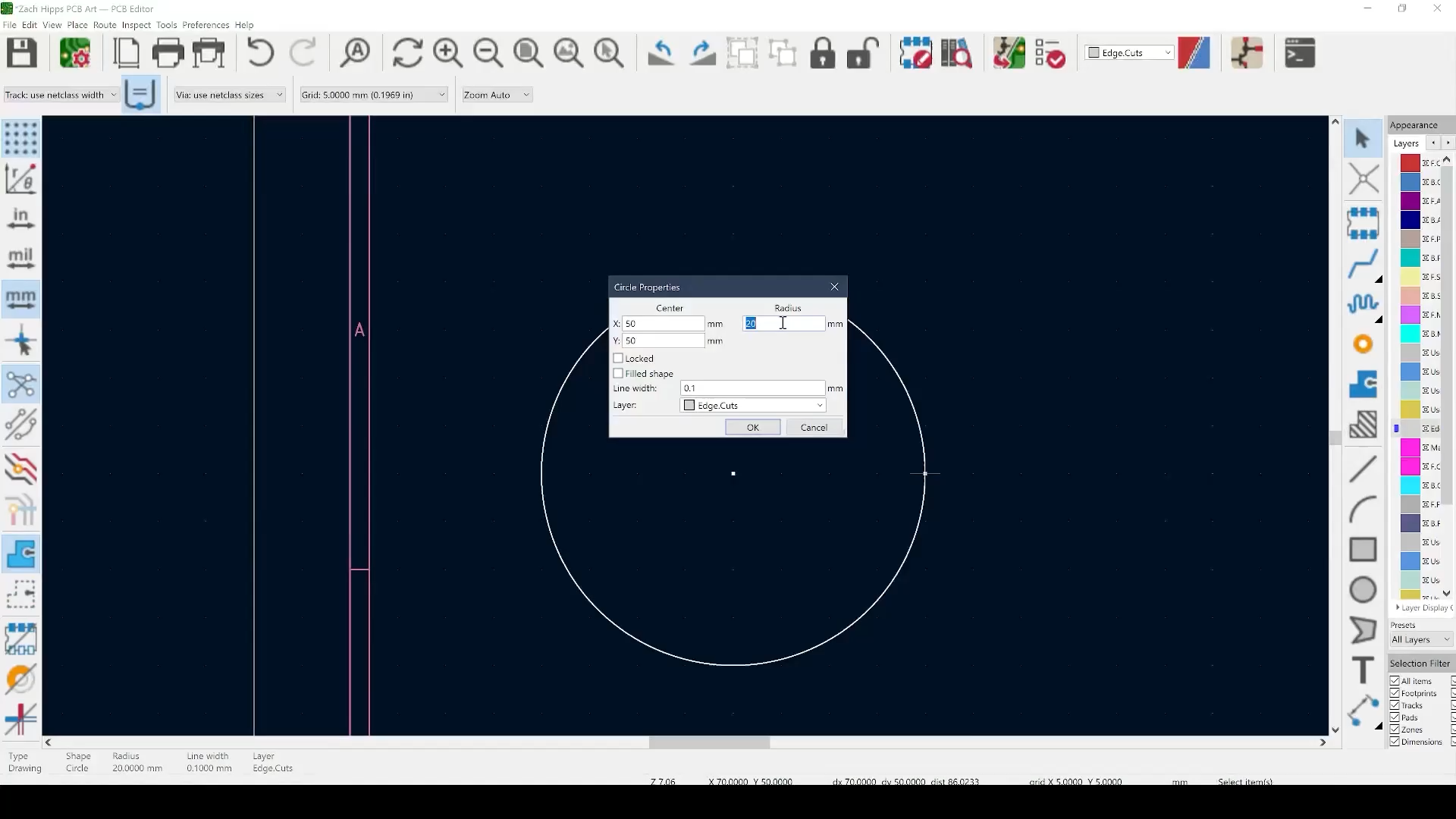
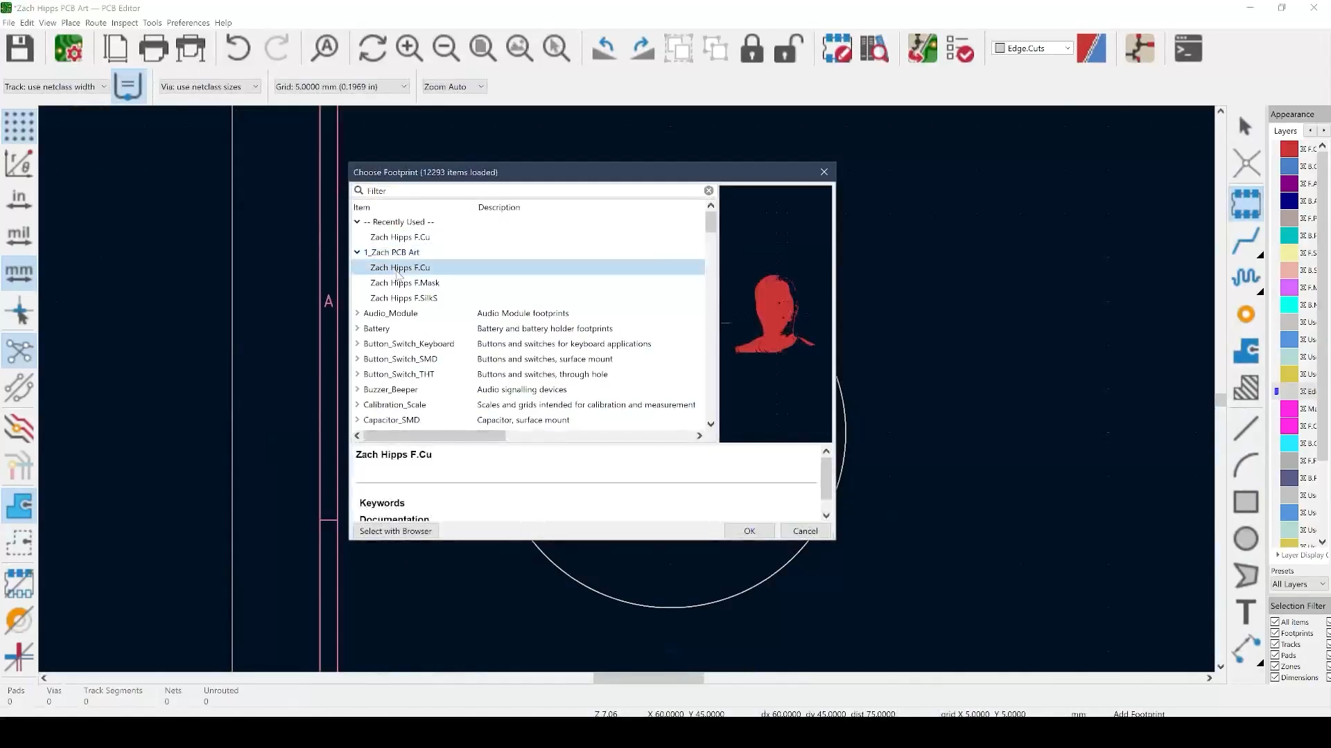
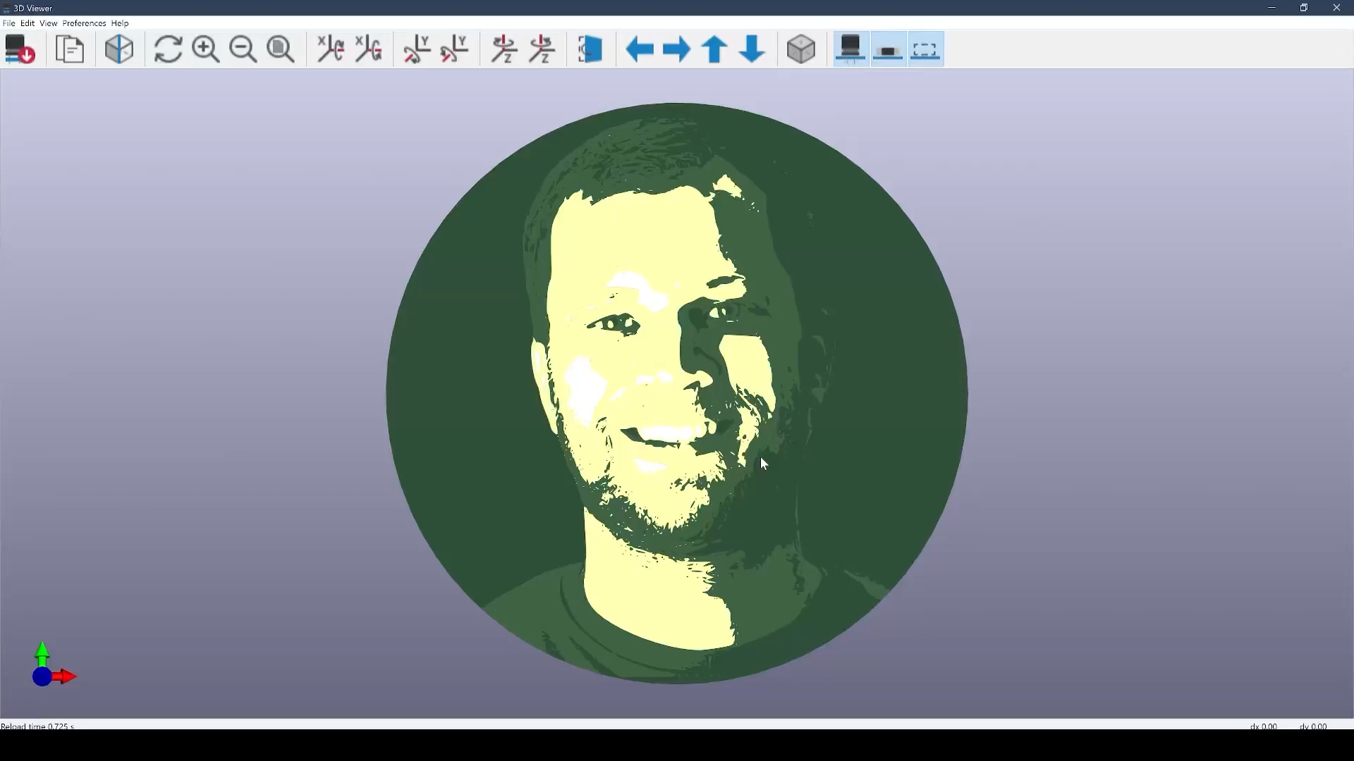
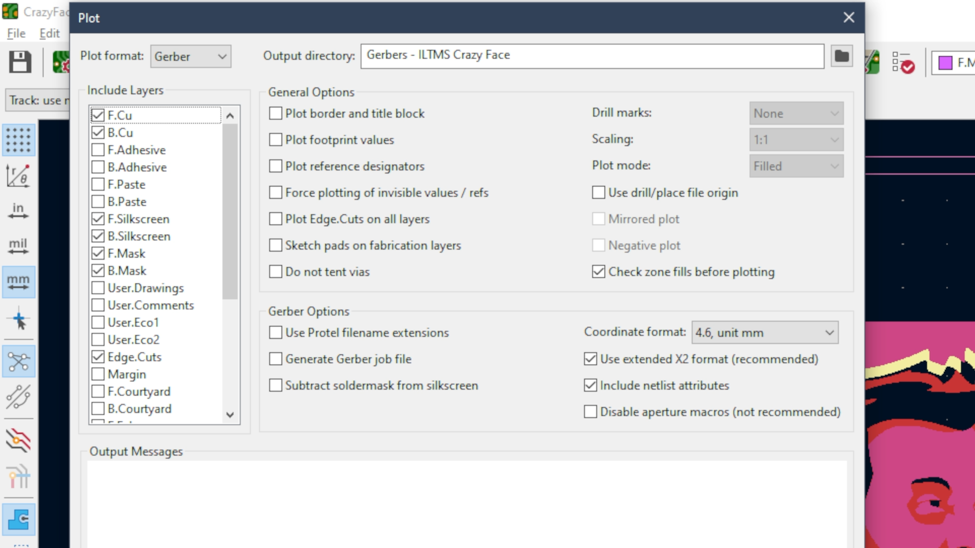
(fp_text reference "G***" (at 0 0) (layer F.SilkS) (effects (font (thickness 0.3))) ) (fp_text value "LOGO" (at 0.75 0) (layer F.SilkS) hide (effects (font (thickness 0.3))) )I don’t want the reference indicator or the word logo to appear on my PCBs so I delete these two elements from all three files. Be careful not to delete anything other than these two elements. They use open and closed parenthesis () to show you where they start and stop. If you accidentally delete something you shouldn’t and can’t get it back with a good ol’ ctrl+z, just use the image converter tool to create the file again. After deleting these unwanted elements I saved all three files. The last thing I need to do is to fix the front copper file. As I teased earlier, KiCad doesn’t have a way to export to the front copper layer so I just used the silk screen layer temporarily. I need to open the front copper file and do a find and replace operation for the whole document. I want to replace every instance of F.SilkS (front silk screen) with F.Cu (front copper). With all that cleanup sorted out, I save the file. Now I’m ready to create the board. First, in the KiCad control panel I create a new project and open “manage footprint libraries” under preferences. Next, I add the path to the layer files I just created in the project specific library tab. I usually add a “1_” at the beginning of the library nickname so that it appears at the top of the list when I go to find the library in the next step. Now I can open the PCB editor tool and create the board outline on the edge cuts layer. My first PCB is going to be a simple circle so I use the drawing tool to create a circle that is 40mm in diameter. I can edit the circle by hovering over any of its anchor points and hitting the letter ‘e’ for edit on my keyboard. This will bring up the properties of the circle. I can edit the size and location of the circle and confirm that it’s on the edge cuts layer of the board. Next I will add a footprint and find the library I just created in the previous step. I place the F.Cu layer at the center of my circle. If I want to see a preview of my PCB I can click on view and 3D viewer to see what my board looks like. Then I will add the front mask and front silk screen footprints I created and see what those look like in the 3D viewer. I want to make sure all the footprints are aligned and centered on the circle outline I created. Once I was happy with the PCB I clicked on plot and selected the three layers from the list and saved them in the gerber format. This is the file format I’ll need to zip up and upload to a board manufacturer’s website to have my PCBs made.
Double Sided Designs and More complex board outlines
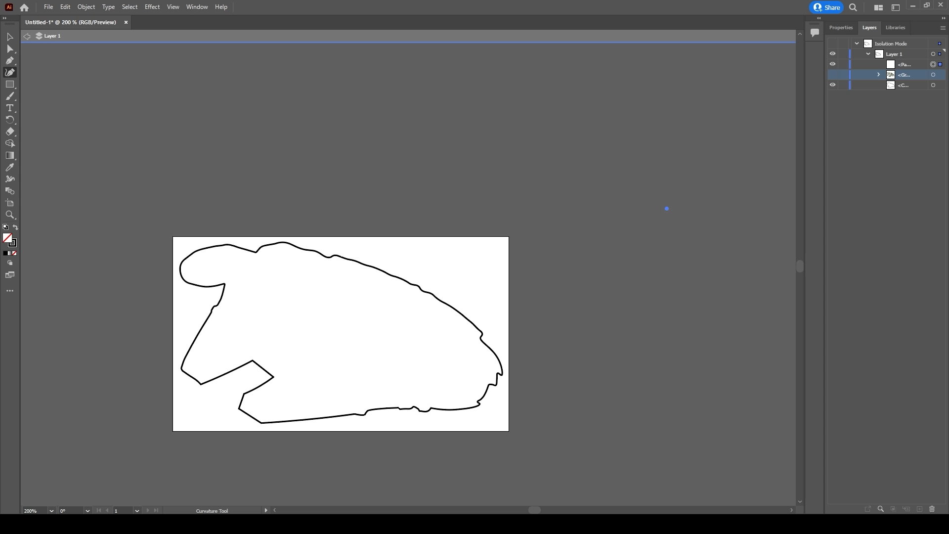
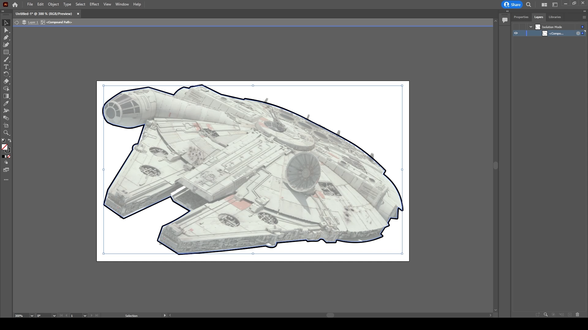
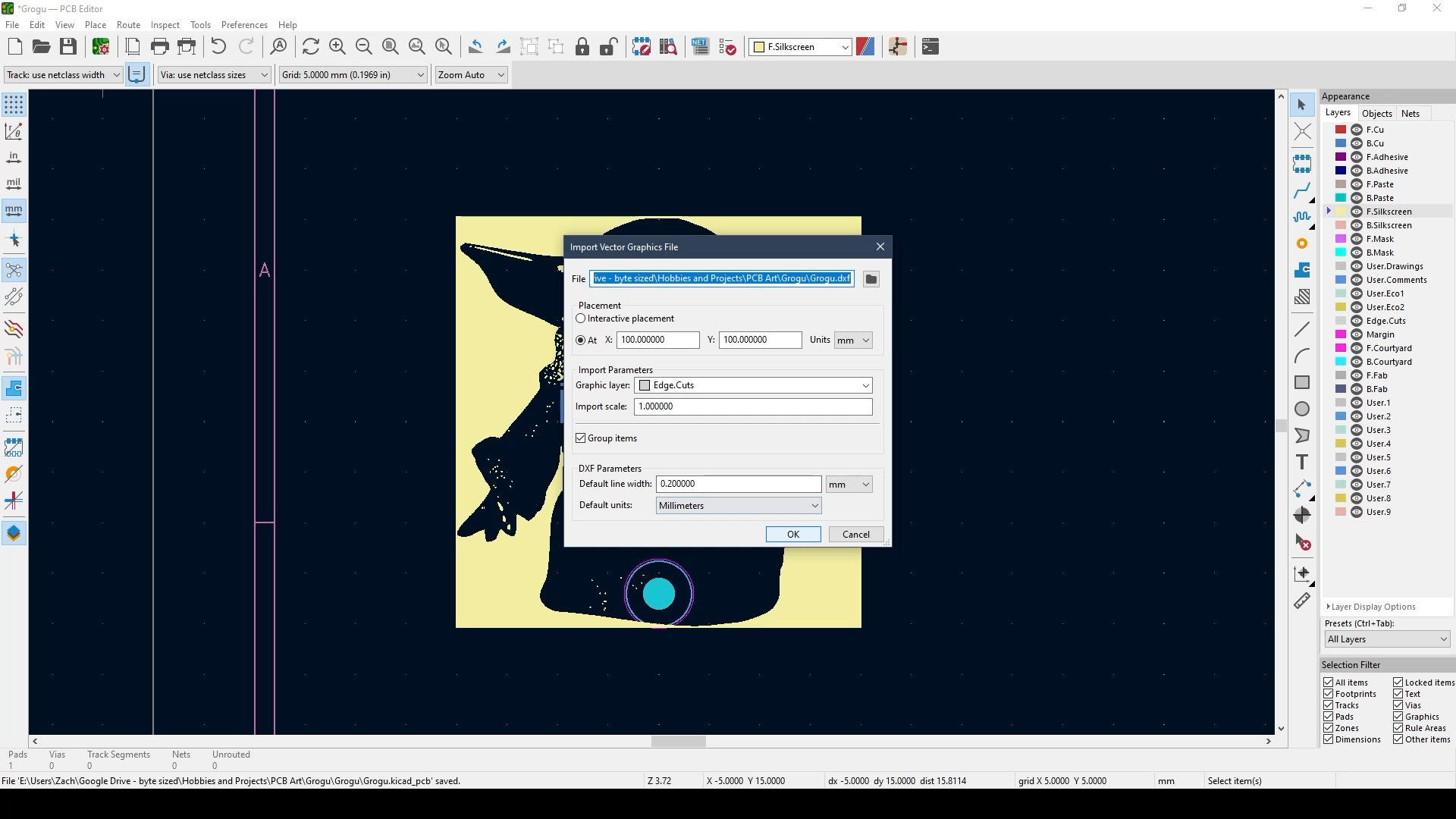
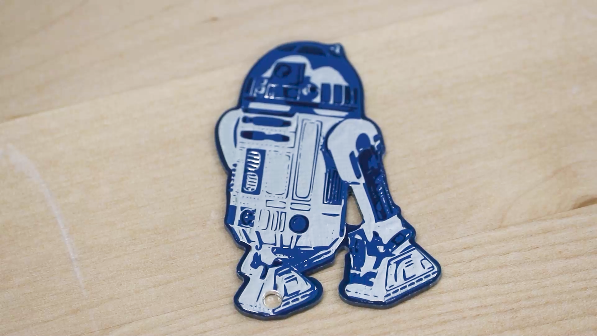
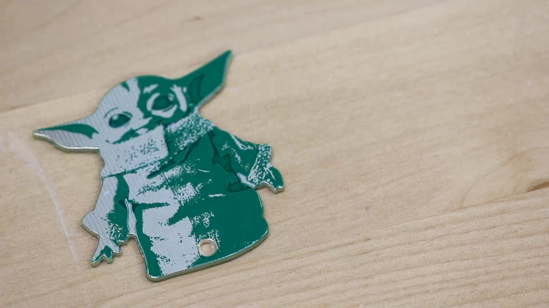
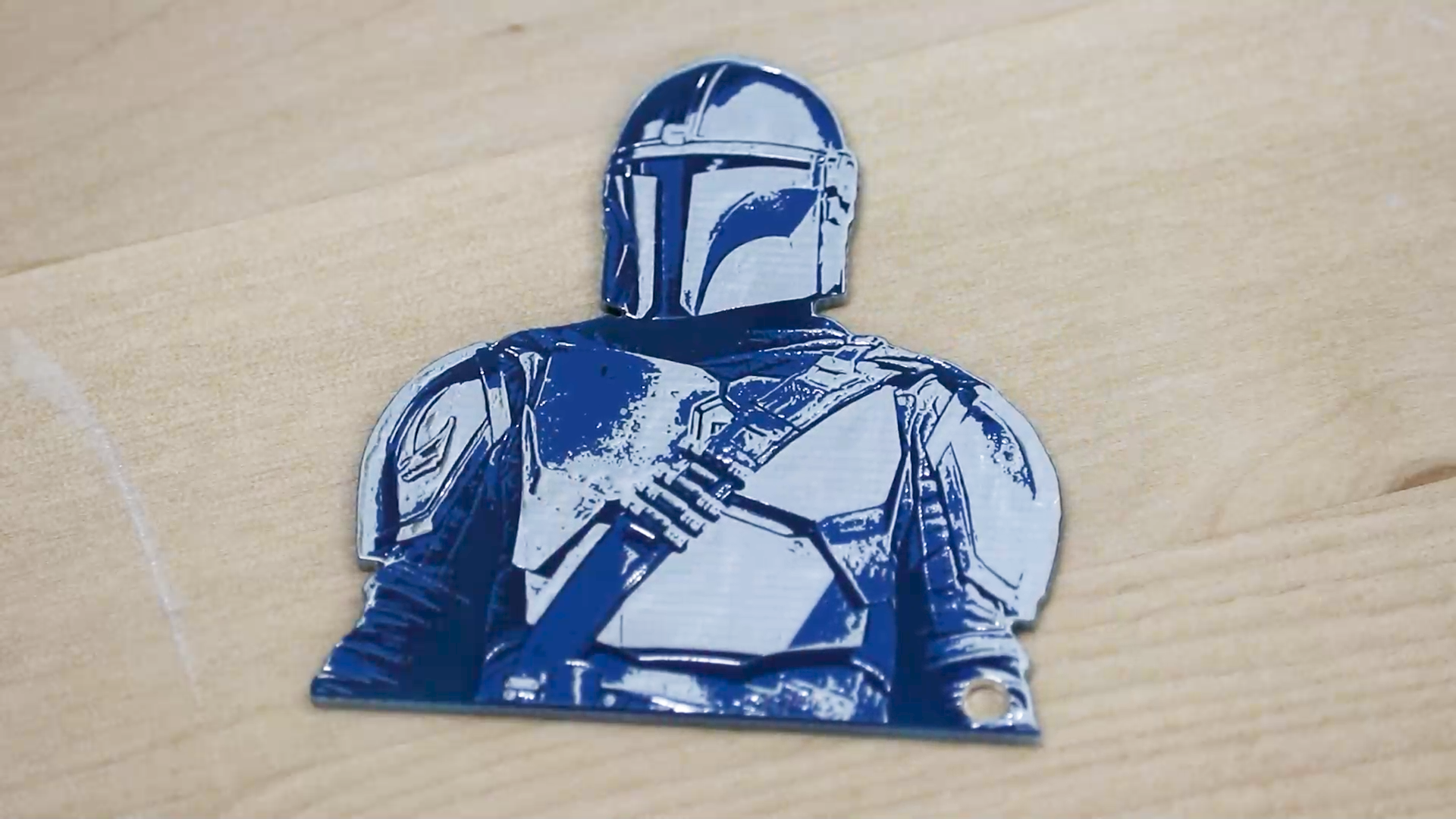
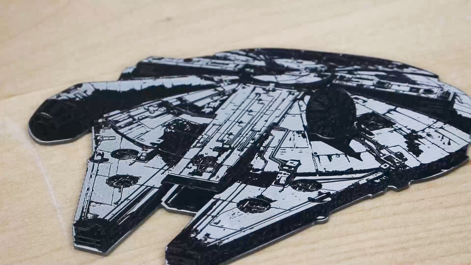
Why have I been using the word “Front” for my copper, mask, and silk screen layer names this whole time? That’s because I can create a totally separate design on the back of my PCBs. I used the same process to put my logo on the back of my PCBs. What happens if I want to create a PCB that isn’t a circle or rectangle? KiCad has an import menu that lets me import a DXF file and use it as the board outline. I used illustrator to do a silhouette image trace on my image. Then I removed the shape fill and just used the shape stroke to create an outline for my boards. I exported the shape as a DXF for import into KiCad.
Lessons Learned
After uploading about 10 different designs to the board manufacturer each one got flagged several times in their automated review process. All of my designs had silk screen being applied on top of tinned copper which would be really bad for a conventional PCB. It would prevent any components from being soldered to that pad. But of course this was intentional for my PCB design because I’m not putting any components on these boards. I told them to please move forward with printed the silk screen on top of the tinned copper but when I received my boards, only a few were done how I designed them. The silk screen was not applied at all to most of the boards I ordered which was really frustrating. I suppose the fix would be to add a note on each layer of the PCB to please add the silk screen on top of these layers. Let them know that the gerber files they are looking at are intentionally done that way. It’s common to add manufacturing notes on each layer, but outside of the board outline and export them right on the gerber file. The other lesson learned was to make sure that my outlines are something that can actually be manufactured. I had a couple of very small and tight corners on my board outlines. Manufacturers use a CNC router to cut around the edge of the board and if the radius is smaller than their end mill, they won’t be able to cut out the board. Each manufacturer will have a page detailing what they are and are not able to do. I would keep corner radii above 1/8” (3mm) unless you are sure the manufacturer can do smaller.